CealTech AS – Endless Possibilities
– posted by Dexter Johnson
Read the article here:
CealTech-AS–Endless-Possibilities
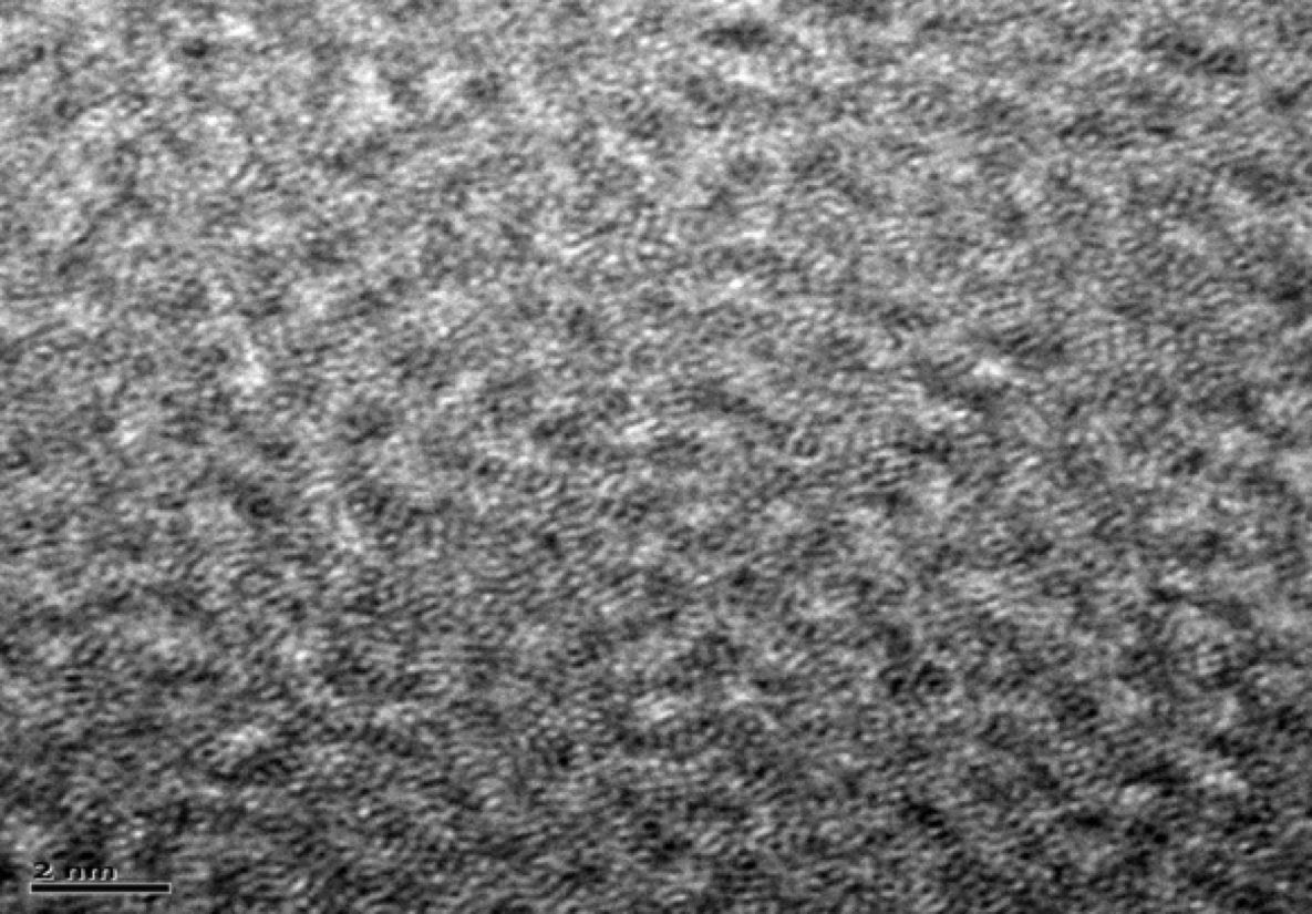
Established in 2012, Norway-based CealTech AS is already staking claim to being the largest volume producer of graphene in the world. This past year, 2016, was a big year in the company’s development with a number of landmark events occurring, perhaps most notably bringing online a new production unit with capacity of 10,000m3 of single layer graphene.
If graphene is going to find use in a more applications, companies like CealTech will undoubtedly play a key role in making that happen by providing high-quality graphene at a competitive price. The company is also moving up the value chain with plans of bringing online this year a large-scale battery production unit that will use graphene on the electrodes.
As the newest member of The Graphene Council’s corporate members we took the opportunity to discuss with them how they see graphene and its applications evolving and how they are positioning themselves in this changing landscape. To do this we spoke with the company’s CEO, Runar Tunem.
Q: Your website makes the claim of having the largest volume production of graphene globally. Can you say what forms of graphene you are producing, i.e. graphene platelets, and how do your volumes breakdown according to those different forms and how they supply your various markets?
A: CealTech produces graphene in powder form. Our graphene is produced by a patented plasma-enhanced chemical vapor deposition (PE-CVD) technology based on DA Boyd, W-H Lin, C-C Hsu, ML Teague, C-C Chen, Y-Y Lo, W-Y Chan, W-B Su, TC Cheng, C-S Chang, et al. Single-step deposition of high-mobility graphene at reduced temperatures. Nature Communications, 6, 2015.
The patent pending FORZA™ production unit makes it possible to produce different types of graphene depending on application. More recently, Dr. David Boyd was able to optimize the process for mass production and the quality of the graphene flakes has been found to be very good. Another advantage of the production unit is that flakes can be directly functionalized according to the intended application, e.g. nitrogen and or oxygen functional groups, without any chemical modification.
Q: In your company’s estimates what is the global production of graphene in all its forms and what percentage of the production does your company represent?
A: Regarding the volumes of graphene, a 28 tons global production was reported in 2010, which is projected to grow to about 575-600 tons by this year. Our estimate lies within the same range for fine- and for ultra-fine graphite. It is important to differentiate between graphite products from graphene’s, as both materials have different properties.
We do expect that the market for pure graphene will grow by leaps and bounds in the coming decade. This will be possible thanks to the advances in manufacturing processes which will address the main challenge of producing large quantities of graphene, in various formats, and at an affordable price, with effective yields and a purity sufficient so as not to impair graphene’s desired chemical properties. In that respect, we believe that CealTech’s technology will be a major enabler, and will contribute to taking graphene to the next level, as we soon start our commercial production of graphene – currently planned from March 2017. CealTech’s expected yearly production volume of pure graphene (from March 2017) is 10,000m3, and this volume will be adjusted (i.e. ramped-up) to accommodate the market needs.
Q: What were the market drivers in demand that spurred your company to make such a large increase in production capacity this year?
A: Over the last couple of years, CealTech has conducted a comprehensive research program aimed at assessing if the use of fine and ultra-fine graphite helped to enhance the properties of a wide range of engineering materials. Examples of the materials investigated by the program are rubber, paints, lacquers, carbon fibers, glass fiber, etc.
During the research program, it became apparent that neither the fine nor the ultra-fine graphite available on today’s market are suitable to attaining such a goal. In comparison, when using the pure graphene produced by our patented PE-CVD technique, we achieved great results by significantly improving the properties of the different materials studied by the program. This learning process was one of the catalysts for CealTech to set sight at becoming the world’s largest manufacturer of PE-CVD graphene.
Q: Going forward what market segments do you see requiring the most volume of graphene? And, what are the markets that will likely exhibit the largest profit margins for graphene producers?
A: The application segments are currently dominated by electronics industry. Due to its high strength and conduction property, graphene is (to be) widely used in this industry. Apart from touch screens for tablets and mobile phones, it can also be used to make circuitry of laptops and personal computers, making them run faster. Also, due to its low thickness, it can be used as a semiconductor. Its chips are faster than the existing silicon chips. The electronics industry is driven by growing demand from the Asia Pacific region and a manufacturing rebound in the U.S. brought on by the economic slowdown of 2007 to 2009. In addition, growing markets for smartphones, tablets, high-definition TVs are further expected to boost the global electronics industry.
Composites accounted for the second largest share (36%) of graphene applications in 2016, dispersed among the automotive, plastics, coatings, construction, metals and engineering materials, aerospace, medical implants and energy markets. These composites can enhance the strength and conductivity of bulk materials. The composites and coatings have also found applications in sports, including lawn tennis and Formula 1 racing.
Looking ahead, Energy Storage and Supercapacitors are expected to emerge as a key area for PE-CVD graphene, followed by composites and graphene coatings. Graphene inks are said to be constantly improving (while their prices seem to be dropping), which might promote, among others, applications like sensor electrodes and smart packaging. Reports project that energy storage will account for around 40%, and composites, 25%, of the market by 2026, and that nearly $100 million worth of graphene will be sold into the energy storage sector in 2026.
Currently, graphene commercialization follows primarily a supplementation/substitution strategy. While products marketed as ‘graphene’ may be on the market in 2016, many, if not all, are still likely (to be) constructed principally from more traditional materials and incorporate a limited quantity of graphite. Accordingly, the profit margins are or will be, to some extent, dictated by the type of graphite used (i.e. quality), and/or the cost of the material that graphene is attempting to substitute. For example, on the low end of the graphene market is bulk material used as a filler to provide strength and conductivity in future day-to-day composite products.
The market for carbon fiber composites was $16,479.4 million in 2013, and was expected to grow at a rate of 12.8% annually from 2014 to 2019 with bulk carbon costs on the order of half-a-dollar per gram. Graphene could replace these products if sold at lower costs. Profit margins on the bulk material are likely to be minimal but significant profits will be made through large volumes. On the other end of the spectrum, the highest quality graphene will be used in applications that are being developed that require graphene, or where the use of high-quality graphene significantly improves the product specifications and performance; hence justifying a premium price. This material will probably command the highest margins –assuming a market structure similar to cell phones. Lithium-ion electrodes are an example where graphite is used as an additive to boost the performance of the electrodes and alleviating a key shortcoming: limited cycle life. In this case, profit margins can be proportional to the degree of improvement enabled by graphene, and as such, could be significantly high.
Q: Do you foresee a business model in which your company will become more involved in downstream production of graphene-enabled products, i.e. moving from producing graphene to producing graphene-enabled products?
A: Further to producing and supplying large volume, high quality PE-CVD Graphene, CealTech is committed to developing and commercializing Graphene-enabled products and solutions for major industries, such as but no limited to: defense, automotive, space & aerospace, energy storage, electronics and sensors, medicine, maritime, and oil & gas. In that respect, our business portfolio is set to encompass everything from Raw Material (i.e. the graphene itself), Manufactured Materials (i.e. graphene doped with oxygen, nitrogen organic and inorganic molecules, etc.), to Component Parts and Finished Products (i.e. battery electrodes, conductive inks, paints and coatings, etc.). On the latter, we are proud to say that we are well on track with the development of a new, revolutionary battery technology. The test results so far are very promising (to be published online soon), and the aim is for an in-house annual production capacity of 20 millions square meters of CealTech’s PE-CVD graphene-based electrodes.
Furthermore, we are working with several leading companies, both nationally in Norway and internationally, to implement our PE-CVD graphene in various industrial products. You will have to stay tuned for more information…
Q: In the mid-2000s, some large chemical companies, like Bayer, drastically increased carbon nanotube production (multi-walled carbon nanotubes) with the idea that the resulting lowered costs of the material would help drive demand. The demand never picked up enough to soak up the increased capacity. What sort of precautions are graphene producers taking to avoid this same kind of pitfall?
A: To answer this, one must try to understand the likely reasons for this ‘pitfall’.
Firstly, one can cite the intrinsic problems of Carbon Nanotubes themselves. In an ideal perfect world, the carbon atoms that form nanotubes should be arranged in a hexagonal network. In this way, each carbon atom is bonded to three other carbon atoms making a sp2 bond, but that is when the nanotubes are perfect and they are of a uniform diameter. However, in reality, there are defects in the nanotubes that cause sp3 bonding to occur. Defects can be observed in the gradual widening or narrowing along the length of nanotubes. Also, nanotubes are not flat, and therefore cannot accurately be modeled with sp2 bond characters. Subsequently, CNTs suffer from lack of control of physical and chemical properties, difficulties in scalability, as well as the high cost of production and purification thus limiting the range of their applications.
In contrast, our produced Graphene with its Sp2 bonding means that the carbon has a ONE double bond. For a carbon with 1 double bond and 2 single bonds, the orbitals will become 33% “s” and 66.7% “p” making our graphene “sp2.” That means that our graphene does not suffer from the same issues as nanotubes as all of our graphene sheets are identical, and therefore its properties are easily reproduced.
Secondly, it is reasonable to say that while some observers believed that the price cut of the MWNT would result in the applications being developed, it was soon recognized that this was a case of putting the cart before the horse, or “technology push” ahead of the preferable “market pull.” In contrast, we see a more downstream-focused approach for the graphene, with the aim of fostering concrete commercial benefits across key industries. As such, significant investments have been made in recent years to hasten the pace at which we start to see more practical applications of graphene and new technologies. For example, the European Union has invested $1.3 billion in ‘The Graphene Flagship’, a consortium of academic and commercial researchers, tasked with taking graphene from the realm of academic laboratories into European society in the space of 10 years, thus generating economic growth, new jobs and new opportunities. Similar efforts are taken by governments across the world (such as USA, China, UK, Japan, South Korea, Singapore, Malaysia, etc.) to build awareness about the vast potential of graphene and to facilitate partnerships and collaborations across the various stakeholders in the ecosystem (e.g., between industry and academia, and/or between upstream and downstream producers). For example, the UK Government has provided £235 million ($353 million) to fund a graphene research center. Tech companies are investing in developing their understanding of the material. Samsung, for example, has already applied for hundreds of graphene-related patents. Furthermore, we see that Graphene producers are also on the ‘offensive’, continuously innovating and developing new technologies aligned to targeted market needs and requirements.
For CealTech’s part, we know that our technology expertise and business strategy address both points above. First, our unique PE-CVD Graphene will be of high quality, produced at large scale, in a reproducible manner, and soon to be commercially available. Accordingly, CealTech is strongly committed to having a resilient and flexible supply chain to ensure fast turnaround times and close customer relationships for its graphene production. Second, we acknowledge the risk of being only in the business of producing a nanomaterial that serves just to make some other product. Therefore, and as mentioned above, we are also focused on developing graphene-enabled products for various industrial applications. We are collaborating with other leading companies to contribute to bringing graphene-enhanced products to the market.
Q: What do you see being some of the graphene-enabled products that are most likely to grow significantly over the next five years and how will that shape graphene production?
A: As stated above, it is expected that graphene continues to be used mainly as a supplementary material in the short term (and through to 2020 at least), until the manufacturing process for graphene is mature enough for it to be used as a key material in products. Barriers to widespread industry uptake mirror carbon nanotubes: functionalization and dispersion; mass manufacturing at an acceptable cost; need for application partnerships; and health and safety issues. So the adoption of graphene and developments of graphene-enabled products depend on how soon these challenges are addressed.
As to which graphene-enabled products are expected to grow the most over the next five years, it is best to refer to interview by the Graphene Council with Prof. Jari Kinaret in his interview – we quote: “The early applications are more likely to use exfoliated graphene flakes than large sheets of graphene. Functional and structural nanocomposites fall in this category – wind power plant blades are one specific example. Other low-hanging fruits are applications where graphene and related materials offer advantages as new or greatly improved functionalities. Here advanced batteries or supercapacitors in anything from portable electric appliances to cars is a promising direction. Also flexible electronics – screens, sensors, smart textiles etc. – are coming strongly. Applications that require large, defect free graphene sheets are likely to take longer time to develop; many solid state electronic applications fall in this category.” We are in perfect agreement with this statement as CealTech and the industry alike, are currently focusing on such products as coatings, batteries, structural composites, functional inks, etc.